Someone at your company has asked how long until they can see the thing working, and you need a number you can defend. So: how long does it take to make a custom PCB in 2026? The design work is the part everyone pictures, and it is almost never the part that eats the calendar. Most of your schedule is queue time, shipping time, and the one respin nobody budgeted for.
The short answer
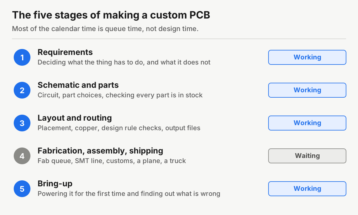
For a simple 2 or 4 layer product with no exotic parts, plan on two to four weeks from "we know what we want" to "it is powered up on the bench." That splits roughly like this:
- Requirements: a day to a week, and it is entirely up to you
- Schematic and parts: hours to weeks, depending on who does it and how long their queue is
- Layout and routing: same, and this is the stage AI tools have compressed the hardest
- Fabrication, assembly and shipping: 4 to 10 days for a small run from an offshore fab, and this floor does not move much no matter what you spend
- Bring-up: an afternoon if it works, a week if it does not
If you get one respin, add another full pass through fabrication and shipping. That is the single biggest swing factor in the whole schedule.
Where the calendar time actually goes
The useful way to look at a hardware schedule is to split every stage into working and waiting. Working time is someone at a keyboard. Waiting time is your files sitting in a queue, your boards sitting on a plane, your parts sitting in a customs warehouse.
Almost everyone estimates the working time and forgets the waiting. Then the schedule slips and it looks like the design took too long, when really the design took two days and the project took five weeks.
Stages 1 and 2: requirements, schematic and parts
Requirements is the cheapest stage to get right and the most expensive to skip. If you have not decided whether this thing runs on a battery or a wall adapter, no one can pick a regulator, and the whole back half of the project is waiting on a conversation you have not had yet.
The schematic and parts stage is where a lot of hidden delay lives, because part availability is not a detail, it is a schedule input. As of the Q2 2026 lead time reports, memory is still the ugly one: Sourceability reports DRAM on allocation at 52 week lead times, with AI-adjacent parts around 40 weeks and some polymer capacitors stretching to 50. Nothing about your 2 layer sensor product is going to hit those numbers, but the lesson carries: a part that is out of stock is not a part, it is a delay, and you should find that out on day two rather than after you place the order.
Practical rule: check stock at your actual assembler before you commit to a part, not at a distributor. If the fab does not have it in their library, you are either shipping it to them or waiting.
Stage 3: layout and routing
This is the stage with the widest spread, because it depends entirely on who is doing it.
Hours-wise, the work itself is not that large for a simple product. CadCrowd puts a single-connector board at as few as 5 to 6 hours, and a complicated one at 360 plus hours, at rates of roughly $95 to $145 an hour for a freelancer. So a simple 2 layer design is not a two-week job in terms of effort. It becomes a two-week job because of the queue in front of it.
Stage 4: fabrication, assembly and shipping
This is the floor, and it is the most predictable number in the whole project.
For bare boards, JLCPCB publishes a 24 hour build time for 5 pieces of a 1 or 2 layer board under 100 by 100mm, 2 to 5 days for the same quantity in 4 layers, and 6 to 7 days for 6 layers. Add assembly and JLCPCB says over 90 percent of assembly orders finish SMT within 24 to 48 hours after fabrication completes, with up to another 48 hours if a part has no existing footprint data in their library.
Then shipping. JLCPCB lists DHL at around 3 to 5 business days, EMS at 7 to 15, and registered airmail at 2 to 4 weeks. The cheap shipping option is where good schedules go to die.
If you would rather keep it domestic, OSH Park quotes 9 to 12 days for standard 2 layer prototypes at $5 per square inch for a set of three, or 4 to 5 business days on their Super Swift service at $10 per square inch, shipping included. They do bare boards only, so assembly is your problem.
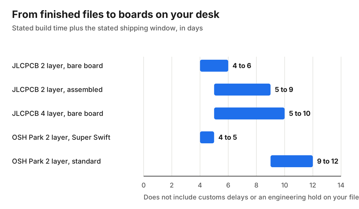
The takeaway: from finished files, about a week is the realistic floor for a small assembled run, and roughly 4 to 6 days if you are soldering it yourself. No design tool changes that. For what each of these steps costs rather than what it takes, we broke the numbers down in how much it costs to make a hardware prototype.
Three timelines for the same simple product
A: your internal EE, or the one you just hired
The design hours are small. The queue is not. An in-house engineer already has a job, and your board joins a list. I cannot give you a verified number for this one because it is entirely specific to your company, which is exactly the point: if you are quoting a date upward, the honest version is "two days of design work, starting whenever Dave finishes the current release." Go find out when that is before you promise anything.
B: an outside design firm
You are buying capacity, and you pay for it. One 2026 pricing guide puts US and UK boutique firms at $180 to $250 an hour, with a simple 2 layer design at $1,500 to $4,000 and a 3 to 7 business day turnaround, and a standard 4 layer at $4,000 to $10,000 over 10 to 14 business days. Quotes typically come back inside 48 hours. Treat those turnarounds as the clock starting after the contract is signed and the kickoff call has happened, which in my experience is a week you should add to the top.
Realistically: 2 to 3 weeks to files for a simple design, plus the fab and shipping week.
C: AI design tools
This is the stage that genuinely collapsed. Describing a simple product and getting a routed board with real, in-stock parts is now a same-session activity rather than a same-month one.
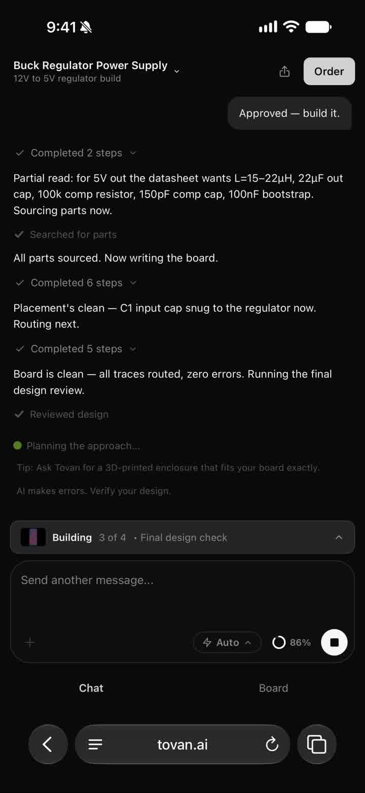
That is a 12V to 5V converter routed in Tovan in a single sitting. Worth being clear about what that does and does not change, though, because it only touches stage 3. The fab week is still the fab week.
The respin is what actually wrecks your schedule
One wrong footprint, one regulator that cannot supply the current, one connector facing the wrong way, and you go back to the design step and repeat every stage after it. The fix might take an hour. Getting corrected boards in your hand takes another full cycle.
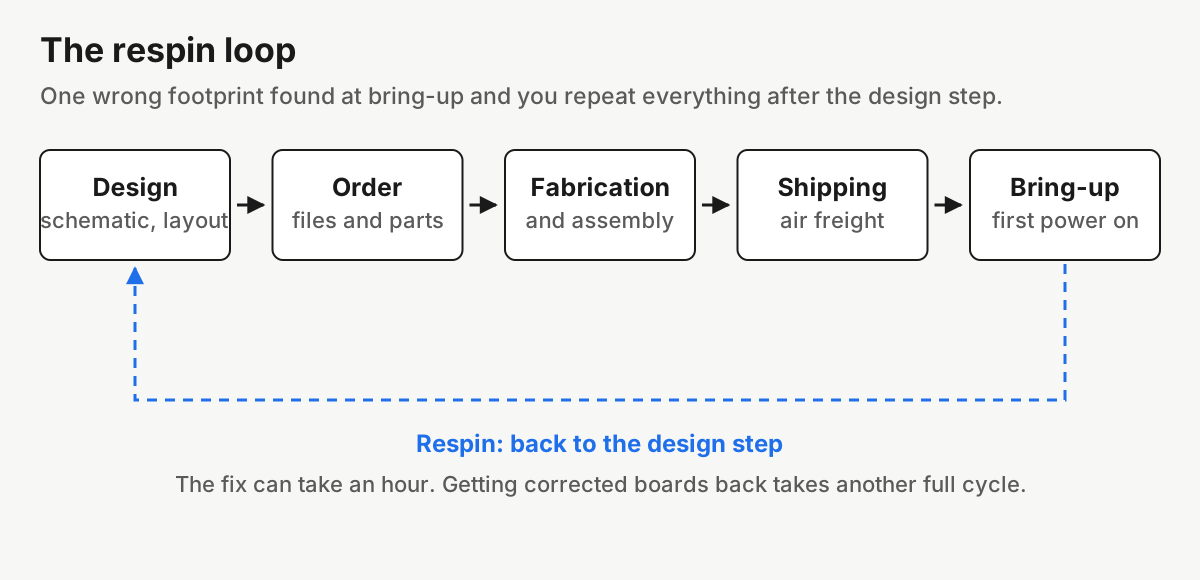
How common is this? For production-grade boards, EMA puts the traditional average at 4.6 design spins to production, against 3.0 with a more modern workflow, and estimates a single complex respin at about four weeks once you count root cause analysis, redesign, fabrication, assembly and validation. Your first simple prototype is not a production program, so do not take 4.6 literally. Take the shape of it: plan for at least one respin, and put it in the schedule you hand your boss.
A two-week project with one respin is a four-week project. A four-week project you promised as two weeks is how you lose credibility with the people funding it.
Stage 5: bring-up
Bring-up is short when it goes well and open-ended when it does not, which is why it belongs in the schedule as a range rather than a day. Power it up in the wrong order and you can destroy the only three you have, which turns an afternoon into another fab cycle.
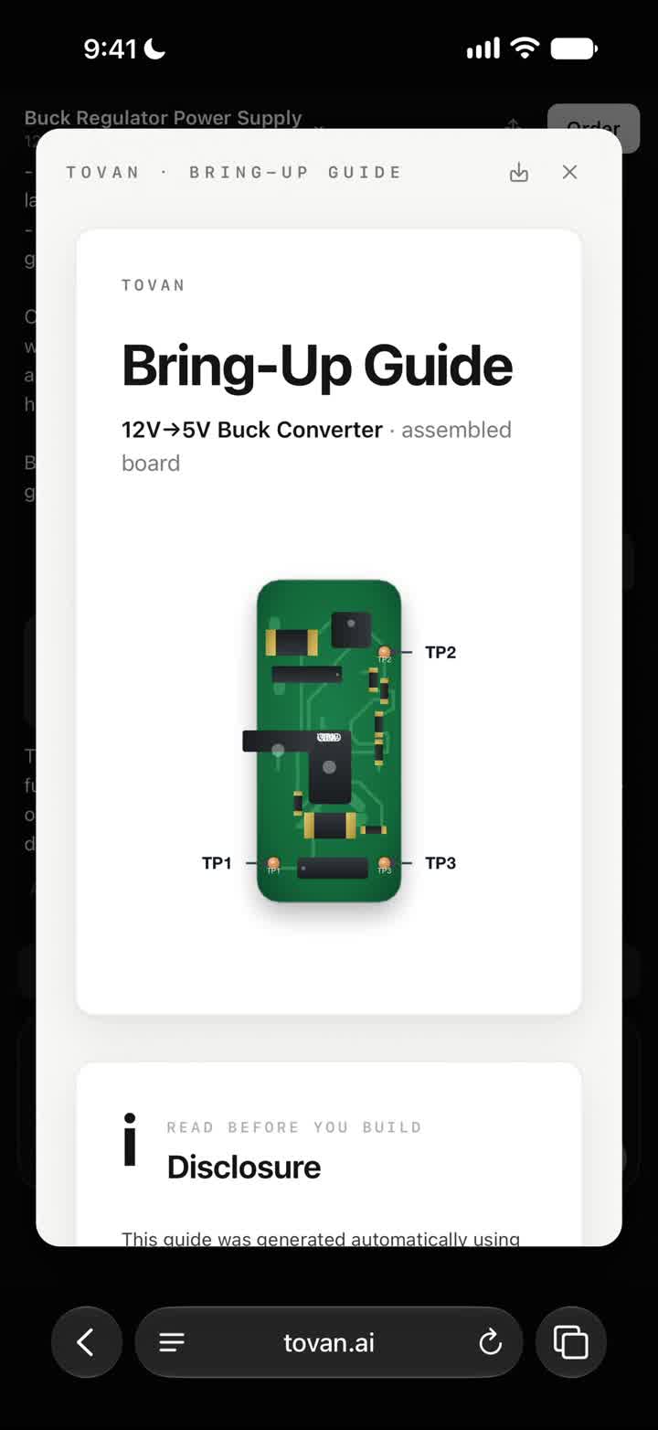
Budget a day, have a plan before you plug anything in, and do the visual inspection first. We wrote up the checklist in what to do when your board arrives.
What compressing the design step buys you, and what it does not
Being honest about this matters more to me than the pitch. Collapsing stage 3 from two weeks to an afternoon does two real things. It removes the queue, so the project starts when you decide it starts. And it makes a respin cheap in engineering time, so the four weeks EMA describes becomes the fab and shipping week plus an hour of fixing.
What it does not do: shorten fabrication, assembly or shipping. (Update, October 2026: it does now write and test your firmware, in beta, which takes a real chunk out of bring-up. Here's how.) It does not help if you are building something high-speed, RF-heavy, or headed for certification, where the schedule is dominated by simulation, test lab bookings and revisions you cannot shortcut. Tovan tops out at 4 layers and is built for the straightforward product, not the hard one. If your project is in that harder category, hire the specialist and plan in months.
And if you are still at the stage of proving the idea works at all, you may not need a custom board yet. Building a proof of concept on a small budget is usually a faster way to answer the risky question.
FAQ
How long does it take to make a custom PCB from scratch?
Two to four weeks is a reasonable plan for a simple 2 or 4 layer product, covering requirements, design, fabrication, assembly, shipping and a first bring-up. Add roughly another week to ten days for each respin.
How fast can I get boards manufactured once my files are done?
JLCPCB publishes 24 hour build times for 5 pieces of a small 1 or 2 layer board, plus 24 to 48 hours for assembly and 3 to 5 business days on DHL. So about 4 to 6 days for bare boards and 5 to 9 for assembled, assuming nothing is flagged in review.
Why does assembly add so much time?
Assembly cannot start until fabrication finishes, and it depends on every part being present and correctly modeled. JLCPCB notes that a part without existing footprint data can add up to another 48 hours just for library creation.
Can I get a custom PCB in one week?
Yes, if the design is already done, the board is 2 layers, the parts are in stock at the assembler, and you pay for express shipping. Every one of those has to be true. Miss any and you are into the second week.
Does paying for expedited fabrication actually help?
A little. JLCPCB sells SMT expedite at roughly $47.83 per day to pull in the estimate, subject to capacity. It buys you a day or two off the build, not off shipping or customs, so it is rarely the best place to spend money if you are trying to save a week.
How long does a PCB respin take?
The design fix is usually fast. The repeat of fabrication, assembly and shipping is the real cost, so plan on the same 4 to 10 days you spent the first time. EMA estimates about four weeks for a complex production board once analysis and validation are included.
If you take one thing from this: the design step is no longer the long pole, so stop estimating the project by it. Count the queue, the fab, the plane, and the respin you are going to have, and the number you hand your boss will be one you can actually hit.
0 comments